
Thiết Kế Phần Cứng
Antenna Tuning Tutorial for Beginners in IoT Applications
Th6
Have you heard about antenna tuning but found the underlying mathematics daunting? This comprehensive guide offers a practical, step-by-step approach to tuning antennas for your IoT devices, enriched with advanced insights and real-world applications.
What is Antenna Tuning?
An antenna possesses resistance, capacitance, and inductance, determined by its physical characteristics—shape, size, material—and the surrounding environment, such as nearby objects or enclosures. When a high-frequency signal is fed to an antenna for radiation, not all power is radiated; a small portion is reflected back to the source due to impedance mismatch. These reflections create standing waves in the transmission line, resulting in power loss. Reflections are minimized when the source impedance matches the load impedance (typically 50 ohms, though other standards like 75 ohms exist in specific applications). Antenna tuning involves adjusting the antenna’s impedance to match the source, maximizing power transfer. If the antenna’s impedance already matches the source, tuning is unnecessary.
Additional Insight: Impedance mismatch can also cause signal distortion, affecting data integrity in high-speed wireless systems. For IoT devices operating in crowded frequency bands (e.g., 2.4 GHz), proper tuning ensures compliance with regulatory standards like FCC or ETSI, avoiding interference with other devices.
Why Tune an Antenna?
The antenna is the cornerstone of any wireless system, handling data transmission and reception at the physical layer. A well-tuned antenna enhances:
- Range: Increases the effective communication distance.
- Power Efficiency: Reduces energy consumption, critical for battery-powered IoT devices.
- Signal Quality: Improves signal-to-noise ratio (SNR), enhancing data reliability.
- Regulatory Compliance: Ensures the device operates within designated frequency bands.
Advanced Benefit: In modern IoT ecosystems, tuned antennas enable robust performance in multipath environments (e.g., urban settings with reflections) and support advanced protocols like LoRa, Zigbee, or Wi-Fi 6, which demand precise frequency alignment.
VSWR, S11, Return Loss
These are key metrics in antenna tuning:
- VSWR (Voltage Standing Wave Ratio): A measure of impedance mismatch, derived from the reflection coefficient (S11 or Return Loss), which quantifies reflected power.
- S11/Return Loss: Expressed in dB, it indicates how much power is reflected back. A lower (more negative) value means better matching.
- VSWR is always positive and real. A VSWR of 1.0 is ideal (no reflection), while VSWR < 2 is considered excellent, as further matching yields diminishing returns.
| VSWR | S11 | Reflected Power (%) | Reflected Power (dB) |
|---|---|---|---|
| 1.0 | 0.000 | 0.00 | -Infinity |
| 1.5 | 0.200 | 4.0 | -14.0 |
| 2.0 | 0.333 | 11.1 | -9.55 |
| 2.5 | 0.429 | 18.4 | -7.36 |
| 3.0 | 0.500 | 25.0 | -6.00 |
| 3.5 | 0.556 | 30.9 | -5.10 |
| 4.0 | 0.600 | 36.0 | -4.44 |
Example: A VSWR of 2 means 11.1% of power is reflected, with 89.9% transmitted. Reducing VSWR to 1.5 increases transmitted power to 96%, a modest gain. For most IoT applications, aiming for VSWR < 2 is practical, as further optimization may not justify the effort.
Added Note: High VSWR can stress RF components, potentially reducing the lifespan of power amplifiers in the transmitter. Monitoring S11 during design also helps identify antenna detuning caused by environmental factors, such as proximity to human hands or metal surfaces.
Antenna Selection
Common Antenna Types
Whip Antenna
- Construction: Simple, widely available with connectors like SMA or U.FL.
- Radiation Pattern: Omnidirectional (donut-shaped, except along the antenna’s axis).
- Pros: High efficiency, plug-and-play with standard connectors.
- Cons: Large size, unsuitable for compact enclosures.
- Use Case: Ideal for external applications like routers or base stations.

Dipole Antenna
- Construction: Simple, no ground plane required.
- Radiation Pattern: Omnidirectional, donut-shaped.
- Variants: Half-wave, monopole, folded dipole, short dipole.
- Cons: Large size limits use in compact devices.
- Use Case: Common in standalone IoT sensors with ample space.

PCB Antenna
- Construction: Compact, integrated into the PCB, tuned by adjusting trace length.
- Pros: Space-efficient, no external matching components needed.
- Cons: Lower efficiency than dipoles; retuning required if PCB changes (e.g., material, thickness).
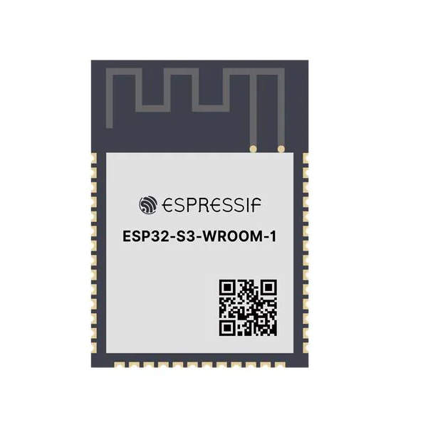
- Use Case: Smartwatches, mobile phones, or compact IoT modules like ESP32.
Dielectric Resonator Antenna (Chip Antenna)
- Construction: Ultra-compact, often requiring a ground plane.
- Radiation Pattern: Near-omnidirectional.
- Cons: Lower efficiency, requires matching circuits that introduce losses.
- Use Case: Wearables, BLE devices, or space-constrained IoT nodes.
New Addition: Ceramic Antennas are gaining popularity in IoT for their small size and ability to operate in high-frequency bands (e.g., 5G or mmWave). They require precise matching but offer robust performance in compact designs.
Some reference Chip antenna can be found here
Working Frequency Range
The antenna’s size dictates its resonant frequency. Larger antennas resonate at lower frequencies (e.g., 900 MHz for LoRa), while smaller ones suit higher frequencies (e.g., 2.4 GHz for Wi-Fi). Select an antenna aligned with your application’s frequency band.
Added Insight: For multiband applications (e.g., dual-band Wi-Fi at 2.4 GHz and 5 GHz), consider multiband antennas or tunable designs to cover multiple ranges without multiple antennas.
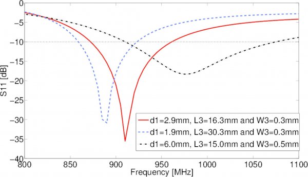
Bandwidth
Bandwidth is the frequency range where VSWR < 2:1 (return loss < -10 dB). For example, a 2.4–2.7 GHz bandwidth suits Wi-Fi/Bluetooth. Antennas in enclosures may experience parameter shifts due to dielectric effects; wide-band antennas mitigate this.
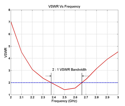
Graph Insight: A comparison of three antennas shows that higher bandwidth (black dotted line) increases return loss, requiring a trade-off. For IoT, prioritize bandwidth if the device operates in dynamic environments (e.g., inside a smart home).
Size and Space Constraints
Smaller antennas incur higher losses. If space permits, use a properly sized antenna. External antennas (e.g., whip) are ideal when enclosures are not required.
Tip: For compact designs, consider PIFA (Planar Inverted-F Antenna), which balances size and performance in mobile devices.
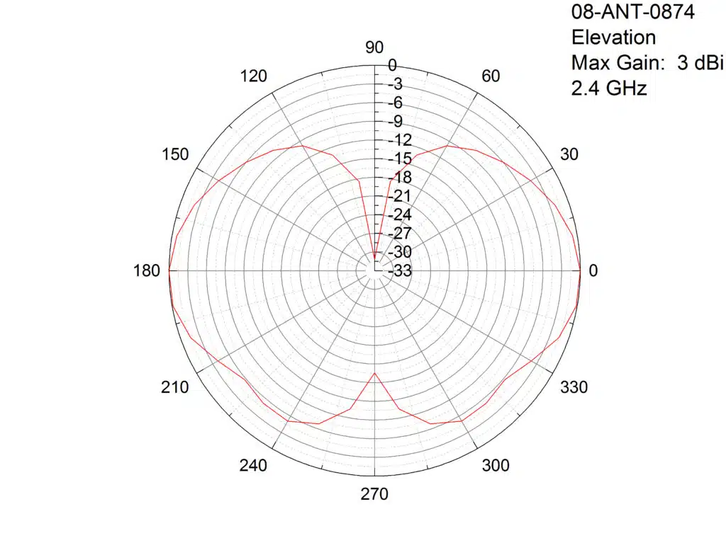
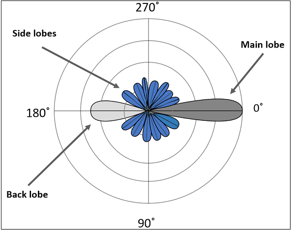
Gain, Radiation Pattern, and Directivity
- High-Directivity Antennas: Offer superior range in specific directions but sacrifice coverage elsewhere.
- Omnidirectional Antennas: Provide uniform coverage at the cost of range.
- Gain: Measured in dBi, positive values indicate better performance than an isotropic antenna, while negative values indicate worse.
- Radiation Pattern: Shows directional radiation with main lobes (strongest) and side lobes (weaker).
Added Concept: Polarization affects antenna performance. Linearly polarized antennas (e.g., vertical) perform best when aligned with the receiver’s polarization. Circular polarization (common in GPS) reduces signal loss in misaligned scenarios.
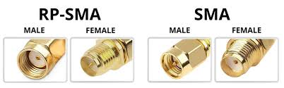
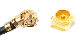
Connector Type
Connectors like SMA or U.FL depend on PCB space and application. MMCX connectors are emerging for compact IoT devices due to their durability and small footprint.
Required Tools
Hardware
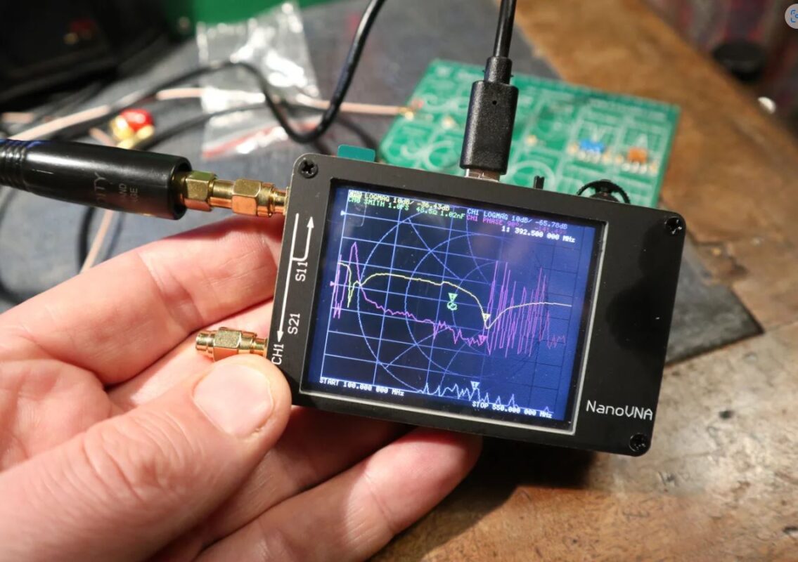
VNA (Vector Network Analyzer)
Affordable options like miniVNA or nanoVNA are USB-based, requiring a computer for visualization. NanoVNA is popular for its portability and open-source software. Purchase link: nanoVNA.
Calibration Kit
Includes short, open, and 50-ohm load standards. Ensure compatibility with your VNA’s connector type (e.g., SMA).
Matching Components
Use inductors and capacitors with low ESR to minimize parasitic effects. Surface-mount components (0402 or 0201) are preferred for high-frequency applications.
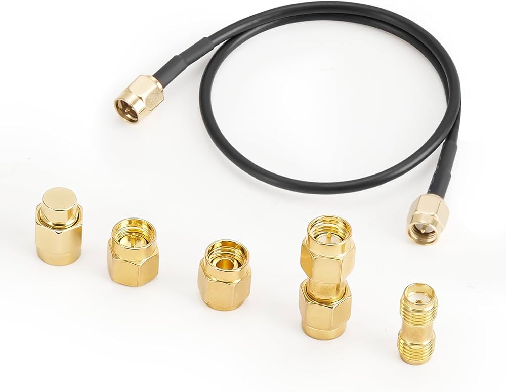
Connector Converters
Adapters like SMA-to-U.FL or SMA male-to-female ensure compatibility between VNA and DUT (Device Under Test).
New Tool: Spectrum Analyzers complement VNAs by measuring radiated power and detecting interference, useful for real-world testing.
Software
VNA Software
VNA-specific software (e.g., nanoVNA Saver) provides advanced analysis like Smith Chart plotting and S-parameter export.
Smith Chart
The Smith Chart visualizes complex impedance, aiding in matching component selection. Tools like SimSmith or RFSim99 simplify calculations. Link: SimSmith.
Added Tool: CST Studio Suite or HFSS for electromagnetic simulation can model antenna performance before prototyping, reducing physical iterations.
PCB Design Guidelines
- Follow the antenna datasheet for placement and clearance.
- Avoid metal objects near the antenna to prevent detuning.
- Match the feedline impedance (e.g., 50 ohms) using a microstrip or coplanar waveguide.
- Include a Pi network (capacitor-inductor-capacitor) before the antenna for tuning, using 0402 components for compactness.
Advanced Tip: Use ground plane stitching (vias) around the antenna to reduce electromagnetic interference (EMI) and improve matching stability.
How to Tune an Antenna
VNA Calibration
Calibration removes systematic errors by measuring short, open, and load standards. Perform calibration close to the DUT to avoid phase errors from long cables.
PCB Calibration
- For standalone antennas, calibrate directly with the kit.
- For PCB-mounted antennas, include the feedline in calibration. Solder a high-quality coaxial cable to the PCB just before the feedline.
- OPEN: Leave the Pi network open.
- SHORT: Short the feedline to ground.
- LOAD: Connect a 50-ohm resistor (1% tolerance) between feedline and ground.
- Save calibration settings for consistency.
Example: For our PCB, we calibrated as follows:
- OPEN: Removed C24, C26, R22, R28, R27.
- SHORT: Placed a 0-ohm resistor at C24.
- LOAD: Installed a 50-ohm resistor at C24.
Tip: Use a calibration plane at the antenna feed point to account for PCB trace effects, ensuring accurate measurements.
Initial Antenna Measurement
Measure the antenna without matching components, ideally in its final enclosure. Check Return Loss and VSWR in the target frequency range. A Return Loss < -10 dB or VSWR < 2:1 is acceptable.
Example: Our initial measurement showed a return loss peak at 2.5 GHz, but the target was the 2.4 GHz ISM band (2400–2483.5 MHz).
Added Note: Measure in both free space and the final environment (e.g., inside a plastic case) to identify detuning effects from nearby materials.
Selecting the Tuning Point
- Single Frequency: Focus on the specific frequency (e.g., 868.5 MHz for LoRa).
- Frequency Range: Target the center frequency (e.g., 2440 MHz for 2.4 GHz ISM) or shift toward higher/lower frequencies based on application needs.
- Use the Smith Chart to locate the target frequency’s impedance. The goal is to move this point to the chart’s center (perfect match).
Example: We targeted 2440 MHz to center the 2.4 GHz ISM band, aiming to align point ‘2’ on the Smith Chart.
Calculating Matching Components
Use tools like SimSmith to determine matching components. Understand Smith Chart movement:
- Series Inductor: Moves clockwise along constant-resistance circles.
- Series Capacitor: Moves counterclockwise along constant-resistance circles.
- Parallel Inductor: Moves counterclockwise along constant-conductance circles.
- Parallel Capacitor: Moves clockwise along constant-conductance circles.
Example: Using SimSmith, we selected an L-network:
- Parallel Capacitor: 1 pF
- Series Inductor: 1 nH
Advanced Technique: For complex mismatches, use a T-network or double-L network to achieve finer control over impedance transformation across wide bandwidths.
Testing with Matching Components
Re-measure with calculated components. If Return Loss < -10 dB at the target frequency, tuning is complete.
Example: Measurements with the 1 pF capacitor and 1 nH inductor showed good performance in the 2.4 GHz band but required optimization for higher frequencies (2480 MHz).
Tip: Account for parasitic effects (e.g., PCB trace capacitance) by slightly adjusting component values during testing.
Iterating for Optimal Tuning
Theoretical calculations may differ from practical results due to parasitic inductance/capacitance. Iterate by adjusting components and re-measuring.
Example:
- Attempt 1: Parallel Capacitor: 1 pF, Series Inductor: 1.5 nH, targeting 2480 MHz.
- Attempt 2: Parallel Capacitor: 0.5 pF, Series Inductor: 1.5 nH, achieving better alignment.
New Strategy: Use machine learning tools like Python-based optimization scripts to predict optimal component values based on VNA data, reducing manual iterations.
Testing in Real-World Conditions
Test the tuned antenna in its intended environment (e.g., inside a case, near walls, or with human interaction).
Example: Pre-tuning, our antenna’s range was ~10 m. Post-tuning, it achieved 90 m line-of-sight and reliable data transmission through two concrete floors at 2 Mbps.
Added Test: Perform over-the-air (OTA) testing using a spectrum analyzer to verify radiated power and check for interference from nearby devices.
Professional Antenna Tuning Services
Need expert assistance for antenna optimization? Contact us for professional tuning and design support tailored to your IoT product!
New Section: Common Pitfalls and Tips
- Pitfall: Ignoring enclosure effects can detune the antenna. Always test in the final configuration.
- Tip: Use 3D electromagnetic simulation (e.g., CST or HFSS) to predict performance before fabrication.
- Pitfall: Poor soldering of matching components can introduce parasitic effects. Use reflow soldering for precision.
- Tip: Maintain a clean RF path by minimizing trace lengths and avoiding sharp bends in feedlines.